- 您现在的位置:买卖IC网 > Sheet目录3861 > PIC18F26K80-I/MM (Microchip Technology)MCU PIC 64KB FLASH 28QFN
PIC18F66K80 FAMILY
DS39977F-page 236
2010-2012 Microchip Technology Inc.
18.1
CTMU Registers
The control registers for the CTMU are:
CTMUCONH
CTMUCONL
CTMUICON
The
CTMUCONH
and
CTMUCONL
registers
(Register 18-1 and Register 18-2) contain control bits
for configuring the CTMU module edge source selec-
tion, edge source polarity selection, edge sequencing,
A/D trigger, analog circuit capacitor discharge and
enables. The CTMUICON register (Register 18-3) has
bits for selecting the current source range and current
source trim.
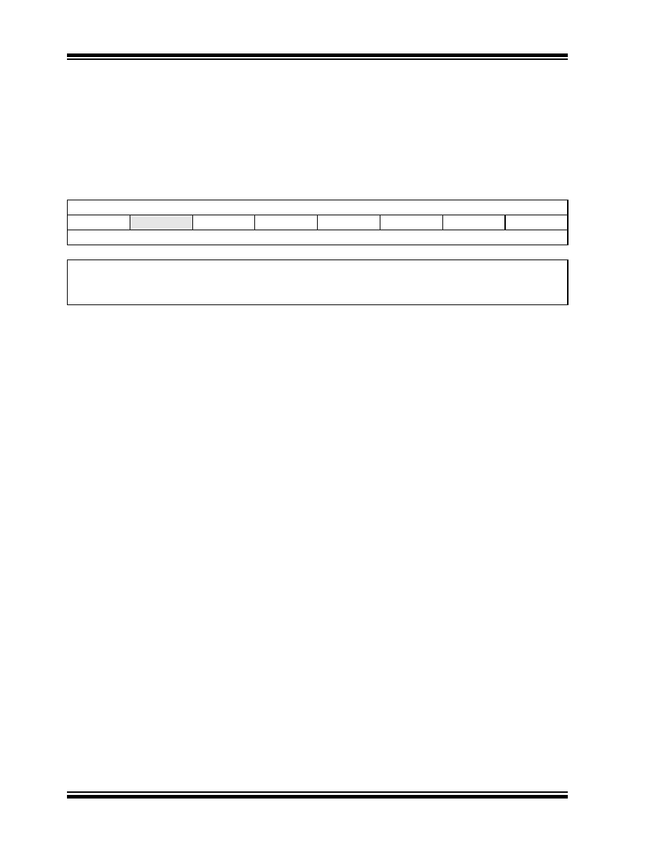
REGISTER 18-1:
CTMUCONH: CTMU CONTROL HIGH REGISTER
R/W-0
U-0
R/W-0
CTMUEN
—
CTMUSIDL
TGEN
EDGEN
EDGSEQEN
IDISSEN
CTTRIG
bit 7
bit 0
Legend:
R = Readable bit
W = Writable bit
U = Unimplemented bit, read as ‘0’
-n = Value at POR
‘1’ = Bit is set
‘0’ = Bit is cleared
x = Bit is unknown
bit 7
CTMUEN:
CTMU Enable bit
1
= Module is enabled
0
= Module is disabled
bit 6
Unimplemented:
Read as ‘0’
bit 5
CTMUSIDL:
Stop in Idle Mode bit
1
= Discontinues module operation when device enters Idle mode
0
= Continues module operation in Idle mode
bit 4
TGEN:
Time Generation Enable bit
1
= Enables edge delay generation
0
= Disables edge delay generation
bit 3
EDGEN:
Edge Enable bit
1
= Edges are not blocked
0
= Edges are blocked
bit 2
ESGSEQEN:
Edge Sequence Enable bit
1
= Edge 1 event must occur before Edge 2 event can occur
0
= No edge sequence is needed
bit 1
IDISSEN:
Analog Current Source Control bit
1
= Analog current source output is grounded
0
= Analog current source output is not grounded
bit 0
CTTRIG:
CTMU Special Event Trigger bit
1
= CTMU Special Event Trigger is enabled
0
= CTMU Special Event Trigger is disabled
发布紧急采购,3分钟左右您将得到回复。
相关PDF资料
PIC16C55-RC/P
IC MCU OTP 512X12 28DIP
SFW23R-2STE1
SFW23R-2STE1-FFC/FPC CONN
PIC24FJ64GA002-E/SS
IC PIC MCU FLASH 64K 28-SSOP
PIC18LF46K22-I/ML
IC PIC MCU 64KB FLASH 44QFN
PIC18F45K80-I/ML
MCU PIC 32KB FLASH 44QFN
PIC24F32KA302-I/ML
MCU 32KB FLASH 2KB RAM 28-QFN
PIC18LF45K80-I/ML
MCU PIC ECAN 32KBFLASH 44QFN
PIC18F4221-I/PT
IC PIC MCU FLASH 2KX16 44TQFP
相关代理商/技术参数
PIC18F26K80-I/SO
功能描述:8位微控制器 -MCU 64KB FL 4KBRM 16MIPS 12bit ADC CTMU RoHS:否 制造商:Silicon Labs 核心:8051 处理器系列:C8051F39x 数据总线宽度:8 bit 最大时钟频率:50 MHz 程序存储器大小:16 KB 数据 RAM 大小:1 KB 片上 ADC:Yes 工作电源电压:1.8 V to 3.6 V 工作温度范围:- 40 C to + 105 C 封装 / 箱体:QFN-20 安装风格:SMD/SMT
PIC18F26K80-I/SP
功能描述:8位微控制器 -MCU 64KB FL 4KBRM 16MIPS 12bit ADC CTMU RoHS:否 制造商:Silicon Labs 核心:8051 处理器系列:C8051F39x 数据总线宽度:8 bit 最大时钟频率:50 MHz 程序存储器大小:16 KB 数据 RAM 大小:1 KB 片上 ADC:Yes 工作电源电压:1.8 V to 3.6 V 工作温度范围:- 40 C to + 105 C 封装 / 箱体:QFN-20 安装风格:SMD/SMT
PIC18F26K80-I/SS
功能描述:8位微控制器 -MCU 64KB FL 4KBRM 16MIPS 12bit ADC CTMU RoHS:否 制造商:Silicon Labs 核心:8051 处理器系列:C8051F39x 数据总线宽度:8 bit 最大时钟频率:50 MHz 程序存储器大小:16 KB 数据 RAM 大小:1 KB 片上 ADC:Yes 工作电源电压:1.8 V to 3.6 V 工作温度范围:- 40 C to + 105 C 封装 / 箱体:QFN-20 安装风格:SMD/SMT
PIC18F26K80T-I/ML
功能描述:8位微控制器 -MCU 64KB FL 4KBRM 16MIPS 12bit ADC CTMU RoHS:否 制造商:Silicon Labs 核心:8051 处理器系列:C8051F39x 数据总线宽度:8 bit 最大时钟频率:50 MHz 程序存储器大小:16 KB 数据 RAM 大小:1 KB 片上 ADC:Yes 工作电源电压:1.8 V to 3.6 V 工作温度范围:- 40 C to + 105 C 封装 / 箱体:QFN-20 安装风格:SMD/SMT
PIC18F26K80T-I/MM
功能描述:8位微控制器 -MCU ECAN 64KB FL 4KBRM 16 MIPS 12b ADC CTMU RoHS:否 制造商:Silicon Labs 核心:8051 处理器系列:C8051F39x 数据总线宽度:8 bit 最大时钟频率:50 MHz 程序存储器大小:16 KB 数据 RAM 大小:1 KB 片上 ADC:Yes 工作电源电压:1.8 V to 3.6 V 工作温度范围:- 40 C to + 105 C 封装 / 箱体:QFN-20 安装风格:SMD/SMT
PIC18F26K80T-I/SO
功能描述:8位微控制器 -MCU 64KB FL 4KBRM 16MIPS 12bit ADC CTMU RoHS:否 制造商:Silicon Labs 核心:8051 处理器系列:C8051F39x 数据总线宽度:8 bit 最大时钟频率:50 MHz 程序存储器大小:16 KB 数据 RAM 大小:1 KB 片上 ADC:Yes 工作电源电压:1.8 V to 3.6 V 工作温度范围:- 40 C to + 105 C 封装 / 箱体:QFN-20 安装风格:SMD/SMT
PIC18F26K80T-I/SS
功能描述:8位微控制器 -MCU 64KB FL 4KBRM 16MIPS 12bit ADC CTMU RoHS:否 制造商:Silicon Labs 核心:8051 处理器系列:C8051F39x 数据总线宽度:8 bit 最大时钟频率:50 MHz 程序存储器大小:16 KB 数据 RAM 大小:1 KB 片上 ADC:Yes 工作电源电压:1.8 V to 3.6 V 工作温度范围:- 40 C to + 105 C 封装 / 箱体:QFN-20 安装风格:SMD/SMT
PIC18F27J13-I/ML
功能描述:8位微控制器 -MCU 128KB Flash 4KB RAM 12MIPS nanoWatt RoHS:否 制造商:Silicon Labs 核心:8051 处理器系列:C8051F39x 数据总线宽度:8 bit 最大时钟频率:50 MHz 程序存储器大小:16 KB 数据 RAM 大小:1 KB 片上 ADC:Yes 工作电源电压:1.8 V to 3.6 V 工作温度范围:- 40 C to + 105 C 封装 / 箱体:QFN-20 安装风格:SMD/SMT